Overview
The Quantum Materials Electron Microscopy Centre (QMEMC) lab is located at the Stewart Blusson Quantum Matter Institute and the Department of Physics & Astronomy at the University of British Columbia.
This unique-in-the-world facility is equipped with an aberration-corrected Bruker Nion HERMES scanning transmission electron microscope (STEM) custom designed to combine atomic imaging with 5 meV energy resolution electron energy loss spectroscopy (EELS).
The system can operate at cryogenic temperatures using a custom side-entry liquid helium cooled sample stage. These capabilities allow probing of the momentum dependence of collective excitations in quantum materials, lattice vibrations, and the spectrum of confined modes in new polaritonic materials.
Research
Electronic and Structural Order
Strongly correlated materials often exhibit ordered states that break the inherent symmetry (translation, rotation, inversion) of the crystal lattice. These symmetry breaking states are entwined with other exotic phenomena like unconventional superconductivity or colossal magnetoresistance, but they remain poorly understood. We aim to directly visualize these order parameters at the atomic scale and map their nanoscale fluctuations.
Collective Excitations
We probe collective electronic and lattice excitations in strongly correlated materials and low dimensional systems. Collective excitations encode key information about the interactions between electrons. We are especially interested in the momentum dependence of electronic excitations and their behavior in correlated matter and low dimensions where exotic electronic and optical modes emerge. This research leverages the 5 meV energy resolution of monochromated STEM.
In Situ Tuning of Electronic Order
Our research program aims to apply external fields to materials in situ and unlock the coupling between order parameters and their conjugate fields. Examples include the application of electric fields and uniaxial strain, which couple to ferroelectric and nematic order, respectively. These measurements are applied inside the electron microscope, allowing the direct visualization of the evolution of domains and fluctuations under external fields.
Positions starting in 2026 are available.
Instruments
Nion HERMES Monochromated STEM
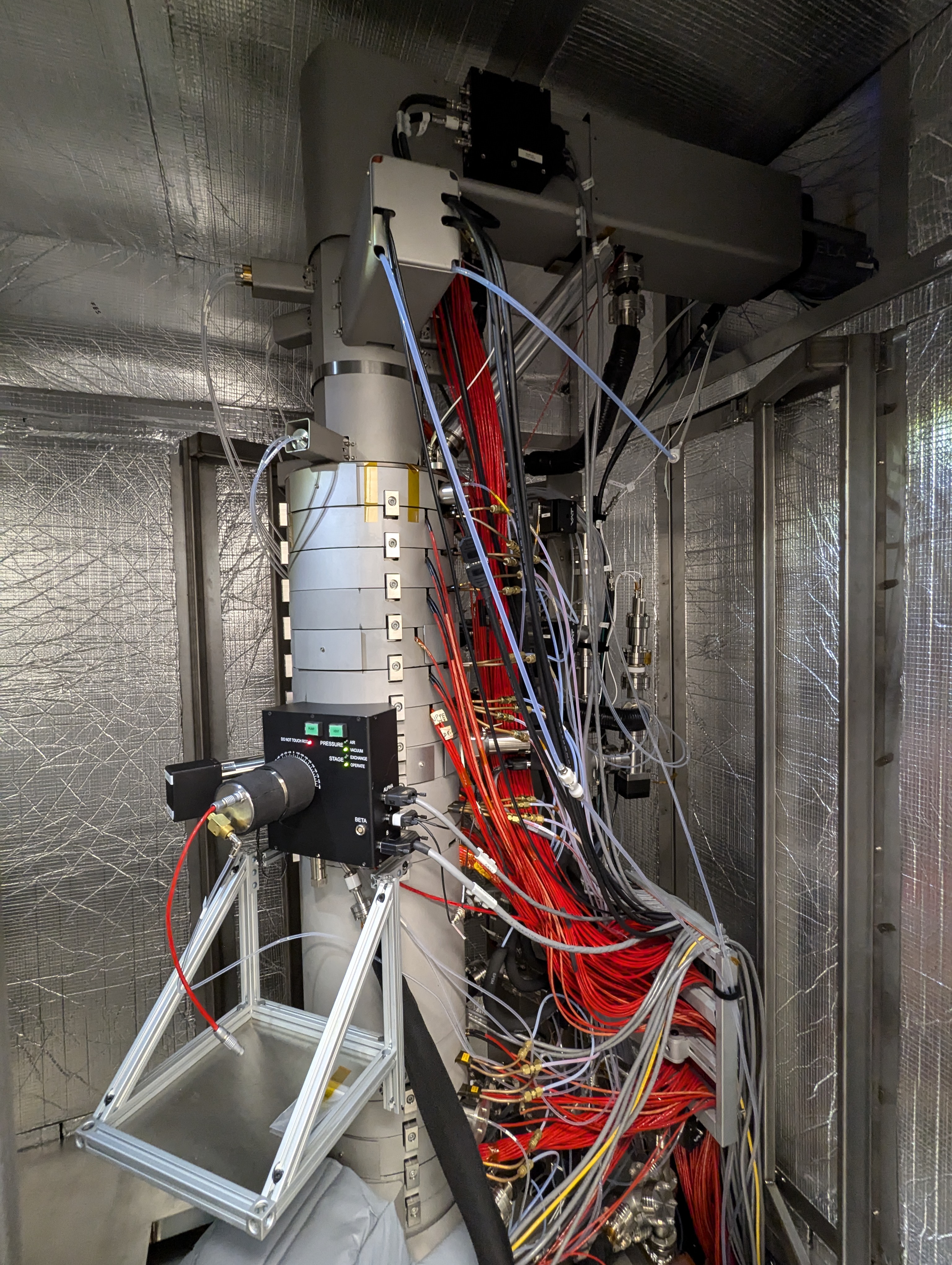
The Bruker Nion High Energy Resolution Monochromated EELS STEM (HERMES) combines a high-brightness cold field emission gun (CFEG) with a state-of-the-art monochromator. The system achieves sub-Angstrom atomic resolution imaging and elemental mapping. The monochromator enables 5 meV energy resolution for spectroscopy in the electron microscope. In addition to spatial resolution, the microscope is optimized to probe the dispersion of collective excitations such as lattice vibrations and plasmons with high momentum resolution.
Focused Ion Beam
The TESCAN Amber Ga+ focused ion beam (FIB) and scanning electron microscope (SEM) enables prepartion of thin TEM samples, microscale device fabrication, and high-resolution ion and electron imaging. The FIB-SEM is equipped with a Pt gas injection system, Autoslicer for automatic lamaella preparation, an electron back-scatter detector (EBSD), an energy dispersive X-ray detector (EDS), and a vacuum transfer module.
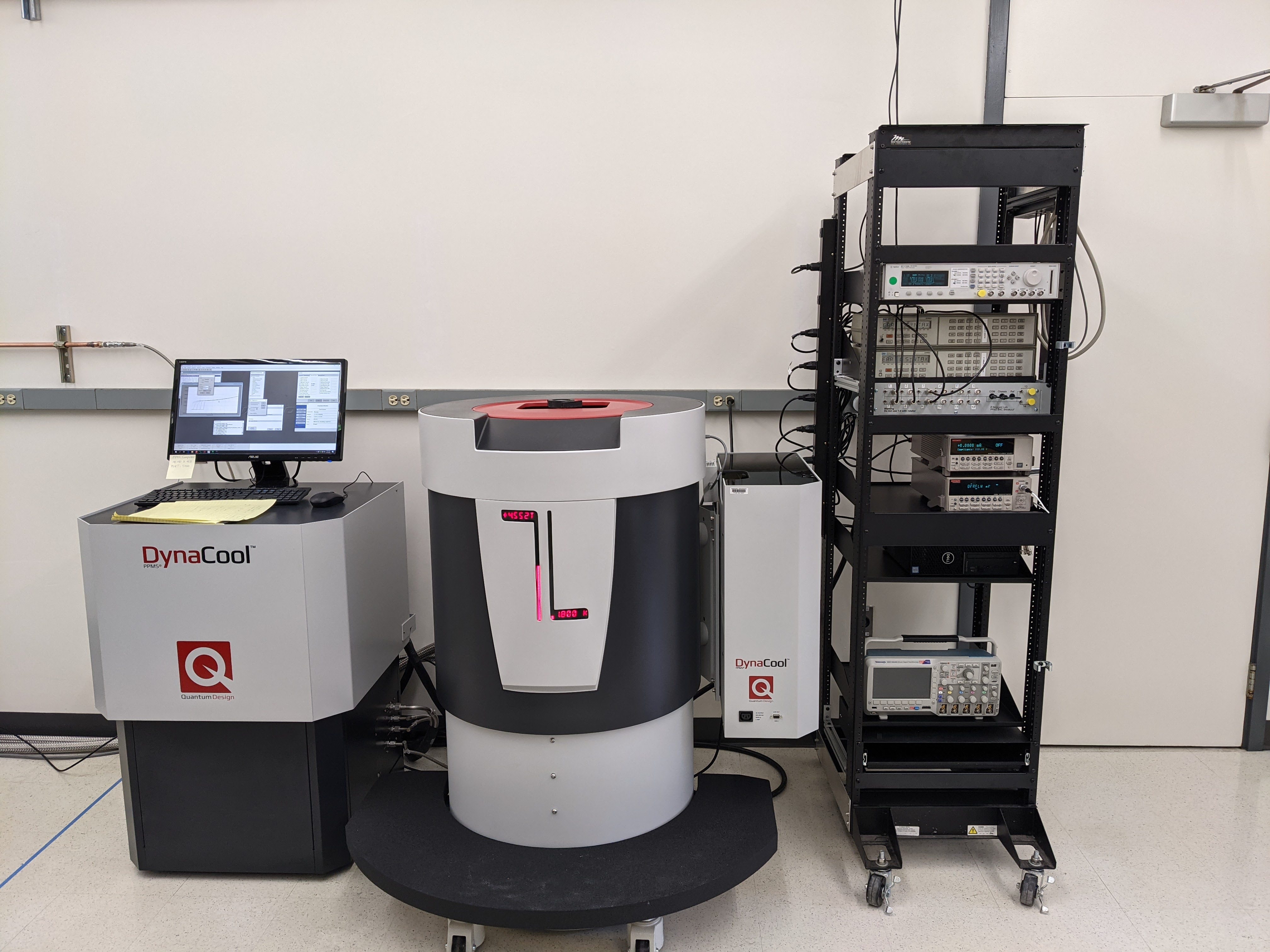
Cryostat Magnet
The Quantum Design Dynacool Physical Property Measurement System enables probing of the electronic transport properties of devices from 1.8 K to 400 K and with magnetic fields reaching 9 T. The system is equipped with a sample rotator, a customizable probe, a Razorbill strain cell with cryogenic insert, and a suite of electronic test equipment.
Other
Ancillary equipment for sample and device fabrication such as wire bonder, diamond saw, ion polishing, 2D transfer station, Allied multi-prep polisher are available.